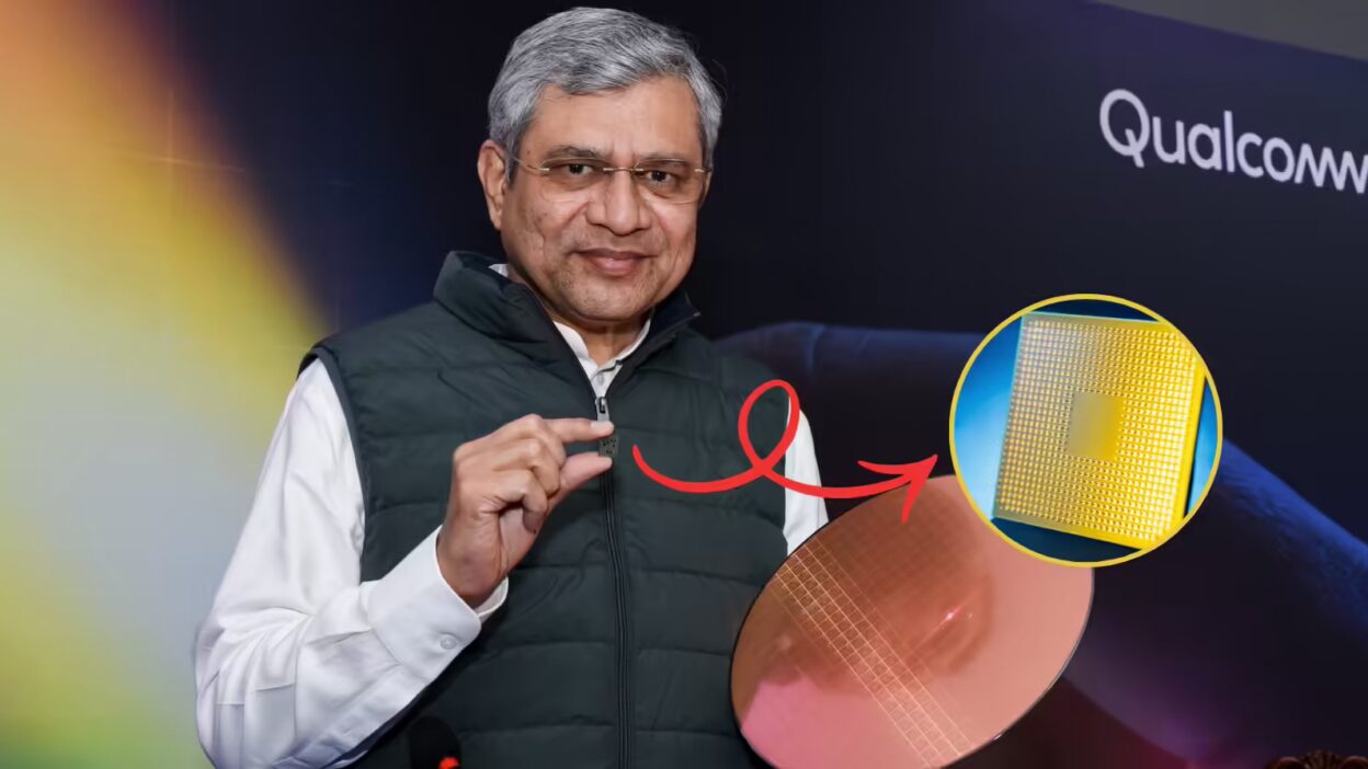
American chipmaker Qualcomm has successfully taped out a 2-nanometer (2nm) chip design from its engineering centers in Bengaluru, Chennai and Hyderabad, marking a significant milestone for India’s semiconductor ambitions.
The company said the advanced chip design was largely developed by its India-based engineering teams, underlining the country’s growing role as a global hub for cutting-edge semiconductor design.
2nm BreakThrough Achieved Through India Engineering Labs
Qualcomm Technologies said on Saturday that the 2nm chip design had been taped out through its India engineering labs in Bengaluru, Chennai and Hyderabad.
The development is being seen as a major boost to India’s semiconductor goals, particularly at a time when the country is seeking to strengthen its presence across the global chip value chain.
The innovation, developed primarily by Qualcomm’s engineering centers in India, further strengthens India’s reputation as a center for advanced chip design, rather than only chip manufacturing.
India Is Qualcomm’s Largest Engineering Base Outside the US
According to Qualcomm, the milestone demonstrates the depth and scale of its engineering presence in India, which is currently the company’s largest outside the United States.
The company said its India teams contribute across multiple areas, including:
- Design implementation and validation
- System-level engineering
- Software platforms and architecture
- Artificial intelligence (AI) optimisation
These teams support global platforms that power billions of devices worldwide, spanning wireless, computing and connected systems.
Government Backs India’s Growing Chip Design Ecosystem

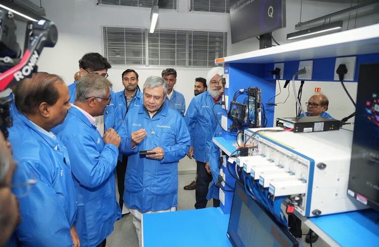
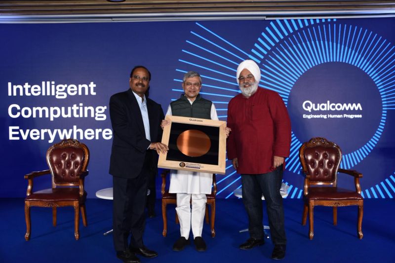
Union Minister for Railways, Information & Broadcasting, and Electronics & IT Ashwini Vaishnaw visited Qualcomm’s Bengaluru facility to mark the achievement.
Commenting on the development, Vaishnaw said India is increasingly playing a central role in shaping future semiconductor technologies. He described the 2nm tape-out as a sign of the growing maturity of India’s chip design ecosystem, in line with the country’s aim of building a globally competitive semiconductor industry.
The 2nm tape-out, according to Srini Maddali, Senior Vice President, Engineering at Qualcomm India, is a confirmation of the nation’s engineering depth. “The greatest personnel is necessary to work closely with global program and architecture teams on advanced semiconductor design, and our India teams routinely deliver at a global standard,” he stated.
The successful 2nm tape-out coincides with India’s increased efforts to establish itself as a global center for semiconductors through business alliances, ecosystem incentives, and legislative support. Qualcomm’s most recent achievement strengthens that drive by indicating that India is increasingly contributing to the design of chips for the future rather than just manufacturing them for the rest of the globe.